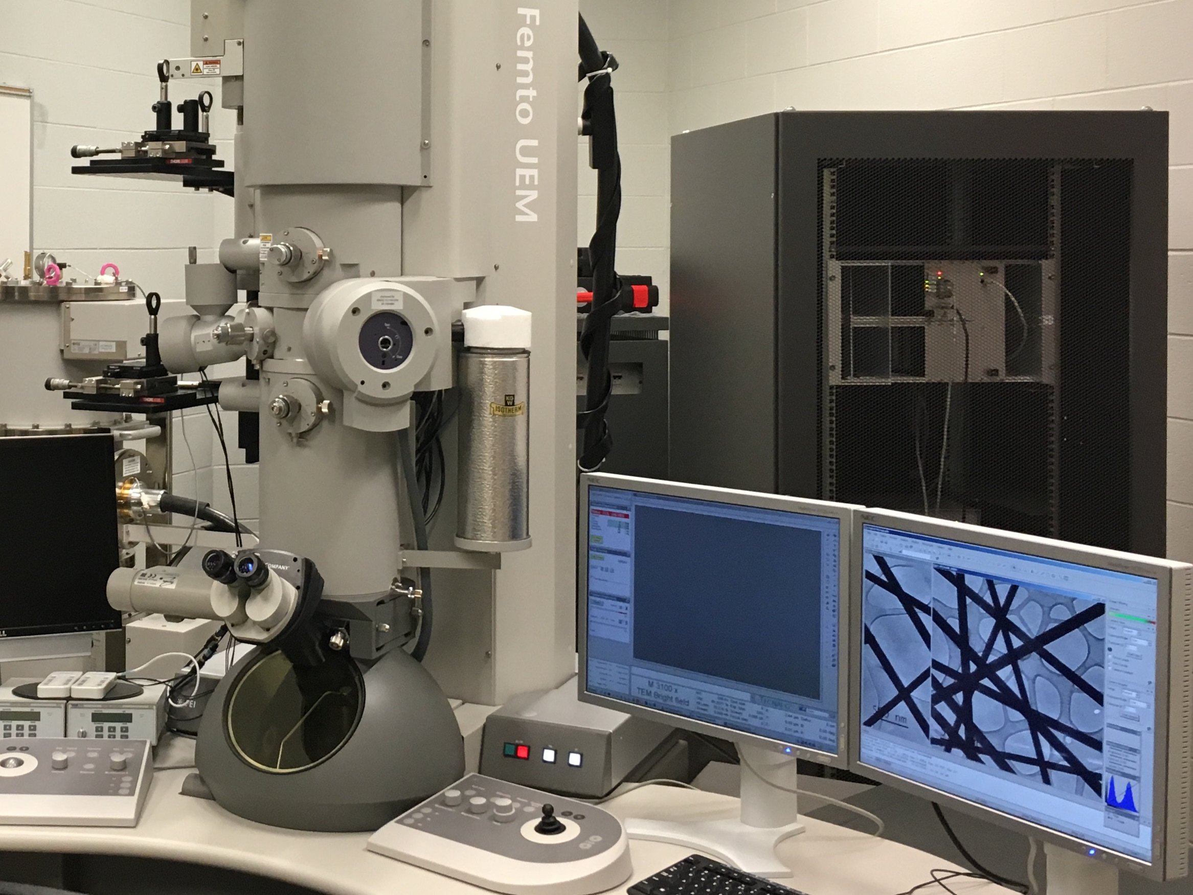
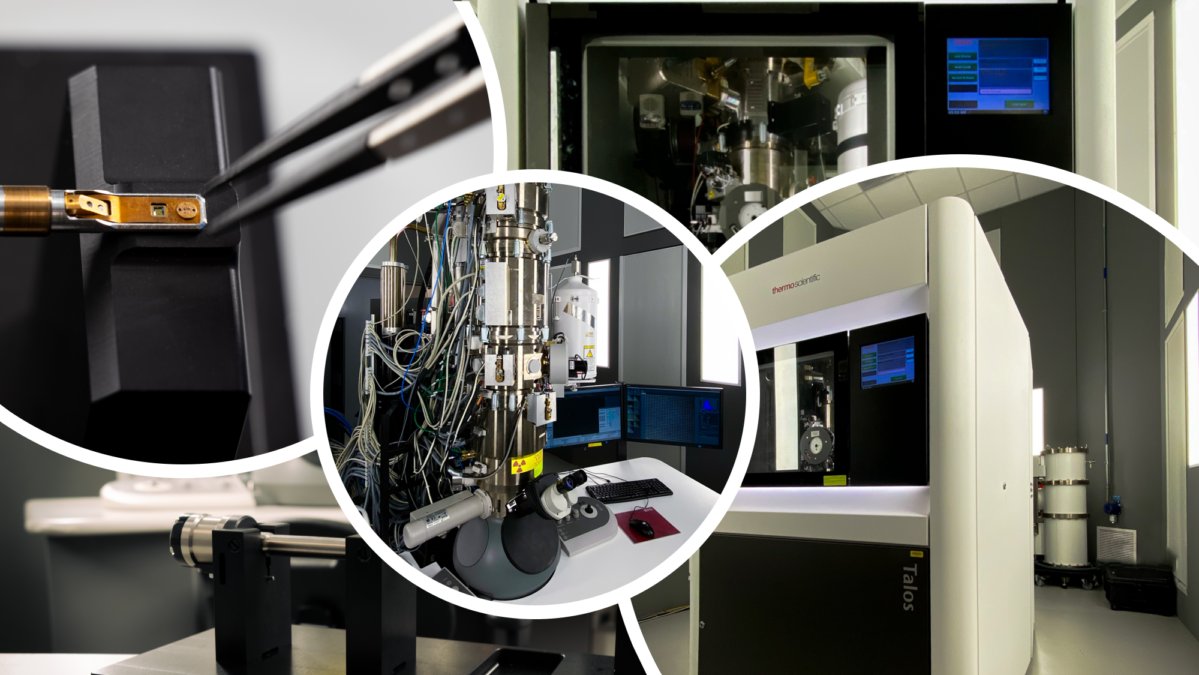
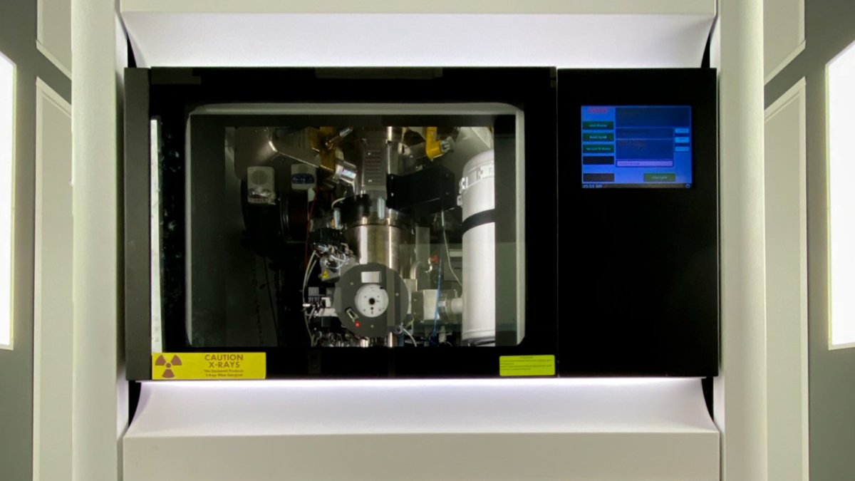
The Ortalan group occupies several labs across UConn Storrs campus. In VORTEX Lab located Edward V.Gant Science Complex, Ultrafast Transmission Electron Microscopy (UTEM) capabilities are developed and applied to achieve new fundamental insights into the origins of dynamic processes seen in the fields ranging from materials science to biology. In-Situ Dynamic Transmission Electron Microscopy and sample preparation by Focused Ion Beam Instruments are performed in the Thermo Fisher Scientific Center for Advanced Microscopy and Materials Analysis (CAMMA) located at the Innovation Partnership Building at UConn Tech Park.
UConn Tech Park also houses a wide variety of fabrication, materials processing and characterization tools including facilities for arc melting, laser sintering, electron beam melting, furnace rheometer, optical dilatometry, elemental analyzer, DSC, ICP, SEM, X-Ray CT, XRD, XRF and TEM. In addition to the instruments in VORTEX Lab, CAMMA and UConn Tech Park, research facilities present in the Institute of Materials Science, are available for advanced materials characterization including GC/MS, GPS, NMR, XPS, AES, SIMS, and Raman Spectroscopy.
Ultrafast Transmission Electron Microscopy Lab
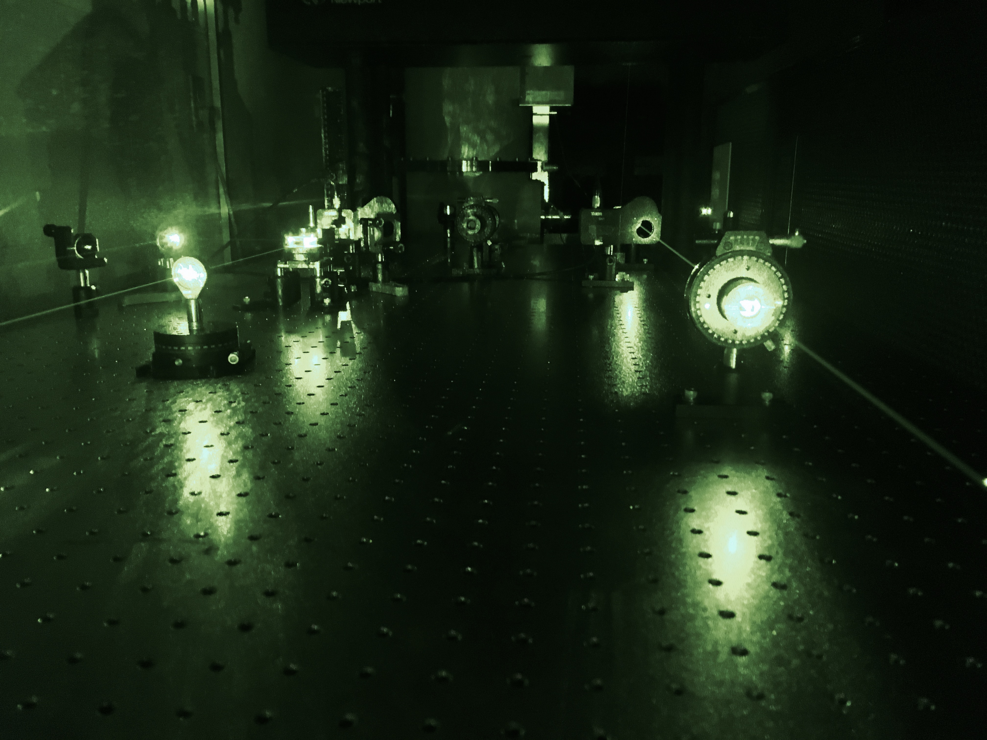
Our UTEM is based on an FEI Tecnai G2 20 system. It has adjustable Wehnelt assembly for various cathode geometries and optics allowing us to operate the microscope in stroboscopic, single-shot and standard thermionic mode with imaging and spectroscopy capabilities and femtosecond time resolution. The microscope has two optical ports providing laser access to the photocathode and specimen. The optical port providing access to the phoelectron generating laser pulse includes a window to bring a 266 nm UV laser pulse into the TEM column. Then, the laser pulse is directed to the photocathode via a mirror to generate the short electron pulse. This electron pulse is accelerated through the electron gun and passes into the electron optics of the TEM column. The electron pulse is then aligned and illuminates specimens as in standard TEM operation, and thus all imaging modes can be utilized, e.g., bright-field, dark-field, selected area electron diffraction. A second optical port provides access to the laser pulse exciting the sample. A pump-probe experiment in the UTEM starts with the excitation of the sample by this sample drive laser pulse, followed by probing the sample with an electron pulse with post-sample lenses set in either diffraction or imaging mode. Several experiments are done with different time delays between the pump and probe, which are used to construct a ‘‘movie’’ of the evolving dynamics of the sample.
In-Situ Transmission Electron Microscopy Lab
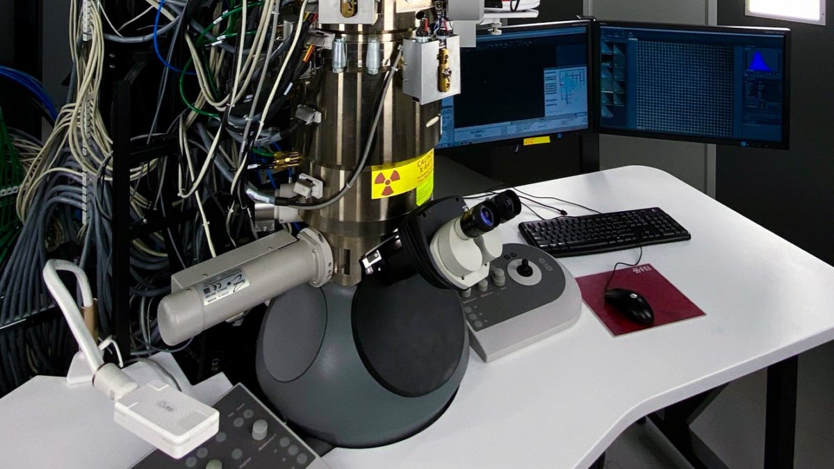
In-situ transmission electron microscopy (TEM) is an area of research, where materials dynamic processes under heat, gas and liquid environment, mechanical stress, and electric/magnetic field are characterized using a transmission electron microscope.
Among various in-situ experiments, the VORTEX group focuses on reactions and transformations under external heat and electric field, experiments in liquid and gas environments, laser-matter interactions, and multimodal approaches. We are equipped with the state-of-art instruments and in situ stages for variety of TEM experiments.
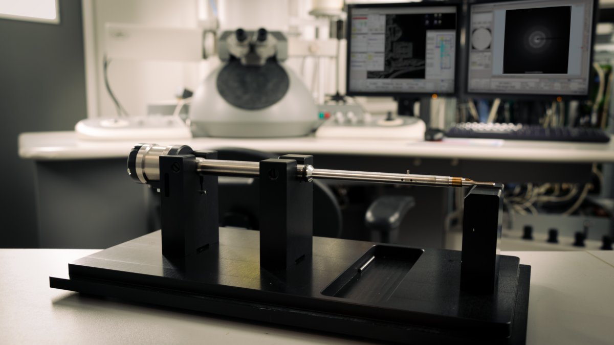
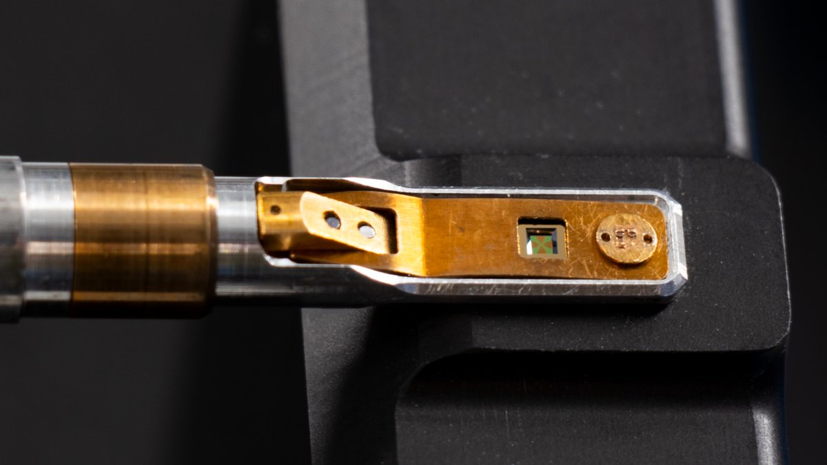
Aberration corrected Titan Themis S/TEM enables atomic resolution imaging of the heat/electric filed induced phenomena. The stimulated reaction/transformation can be monitored real-time with high stability, low drift and high resolution through FEI MEMs-based NanoEx-i/v holder.
Detailed specifications are:
Aberration Corrected Titan Themis:
Operating voltage: 60 ~ 300 kV
Imaging mode: TEM or STEM
Resolution: down to 63 pm in STEM at 300 kV
Energy Filtered CCD and EEL Spectrometer: Gatan Image Filter Quantum SE/963 P (2kx2k)
X-ray EDS detector: Super X Detector (4 Silicon Drift Detectors)
HAADF detector: Fischione 3000 annular detector
Maximum specimen tilt: - 80 to 80 degree tomography holder
Holders: Single-tilt, double-tilt, tomography holder, FEI MEMs-based NanoEx-i/v heating/biasing holder, and in-situ Poseidon Select liquid flow holder
Ion and X-Ray Microscopy Lab
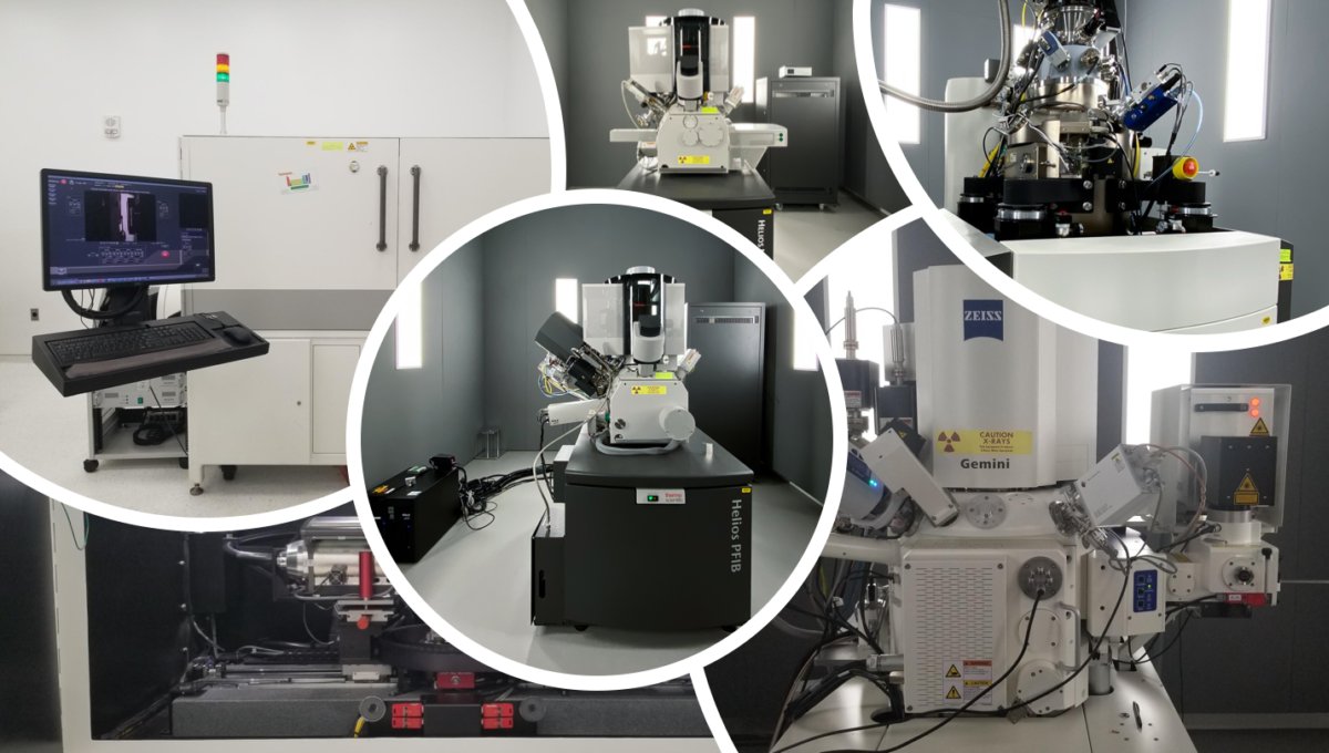
Focused Ion Beam (FIB) is a technology that utilizes an accelerated beam of ions for imaging, materials removal, and materials deposition at a size scale of a few microns to a few nanometers. In VORTEX group, we use several Dual Beam FIB systems with different ion sources like Gallium, Xenon and Neon to process semiconductor materials, prepare TEM sample, design and fabricate various nanostructures for a specific use.
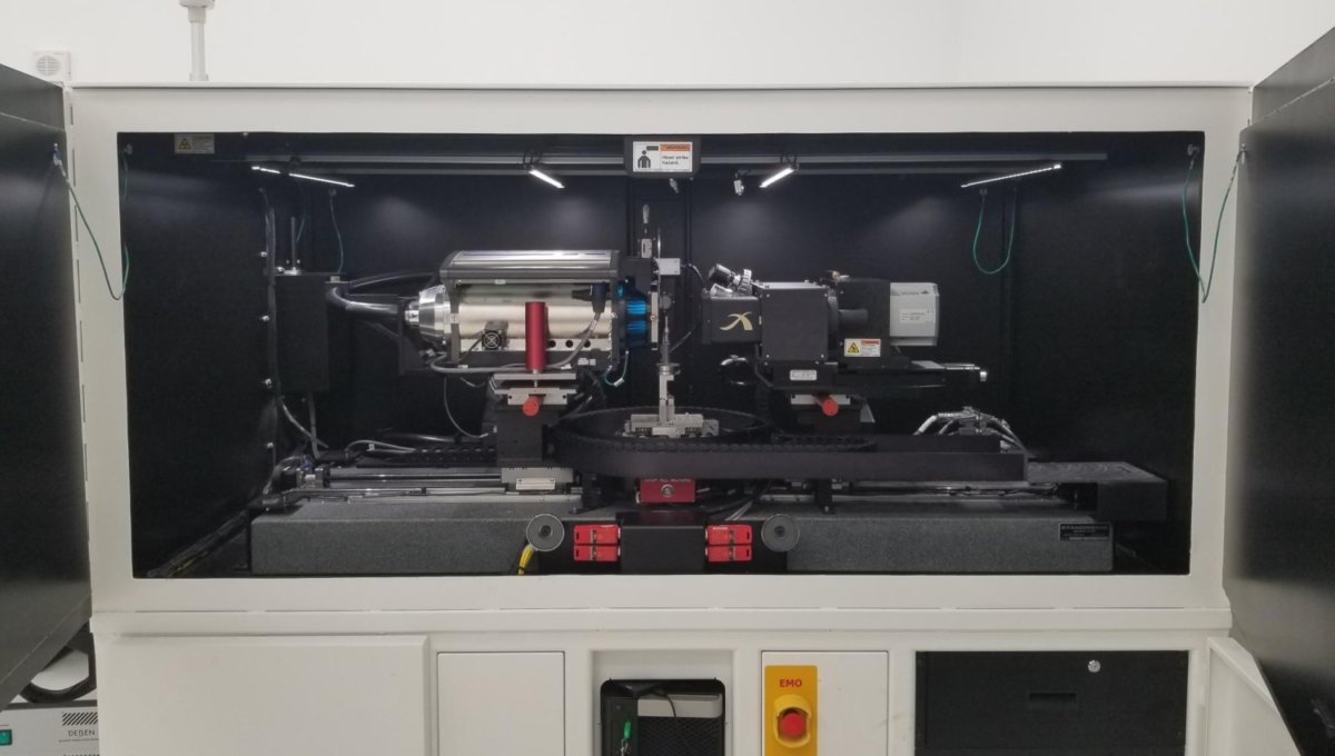
The Micro-CT (Computed Tomography) instruments utilize x-rays to obtain slice by slice information for non-destructive visualization and analysis of the internal structure of materials. The instrument provides 3D tomograms of the samples at submicron resolutions. The instruments is equipped with in situ capabilities and a variety of filters to tune the x-ray energy spectrum. The VORTEX group uses this technology to study the internal structure of materials and the distribution of various microstructures and defects.
Detailed specifications are:
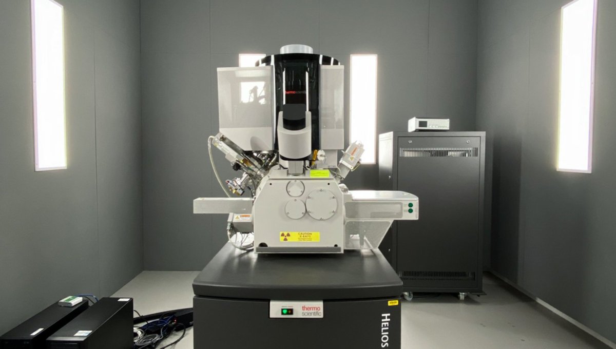
Helios 460F1 Dual Beam:
Gallium Ion milling and high resolution SEM
Electron beam current range: 0.8 pA to 100 nA, accelerating voltage range: 200 V - 30 kV
Ion beam current range: 1 pA to 65 nA, accelerating voltage range: 500 V - 30 kV
Detectors: TLD-SE, TLD-BSE, ETD, ICE, Retractable STEM detector with BF/DF/HAADF segments
Rotation: 360 degree, Tilt Range: -10 to + 60 degree
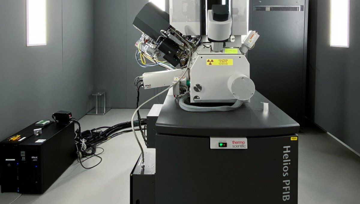
Helios PFIB Dual Beam:
Xenon ion volume milling and SEM
High performance PFIB column with Inductively Coupled Xe+ Plasma (ICP)
High-stability Schottky field emission gun to provide stable high-resolution analytic currents
Electron beam current range: 0.8 pA to 100 nA, accelerating voltage range: 200 V - 30 kV
Ion beam current range: 1.5 pA to 2.5 uA, accelerating voltage range: 500 V - 30 kV
Detectors: TLD-SE, TLD-BSE, ICD, Rotation: 360 degree, Tilt Range: -38 to + 60 degree
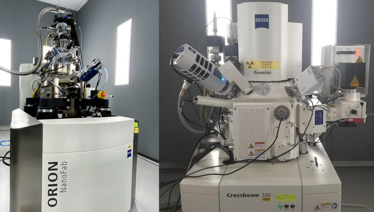
Zeiss Orion Nanofab:
Gas Field Ion Source (GFIS) and column including helium and neon source gas operation
Helium Ion Beam: Resolution: 0.5 nm@30 kV, Beam Energy: 10-30 kV, Beam Current: 0.1 to 100 pA
Neon Ion Beam: Resolution: 1.9 nm@25 kV, Beam Energy: 10-25 kV, Beam Current: 0.1 to 50 pA
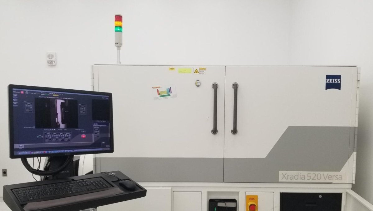
Zeiss 520 Versa X-ray Microscope:
Spatial resolution: 0.7 micrometers, Minimum Achievable Voxel: 70 nm
Tube Voltage Range: 30-160kV, Maximum Output: 10 W
Detector with multiple objectives (0.4x, 4x, 20x magnifications) with optimized scintillators

