Recent developments in instrumentation have made it a very exciting time to perform both fundamental and applied research in the electron microscope. Aberration correctors have taken spatial resolution below the 1 angstrom barrier for inorganic materials and promise to do the same for organic/biological materials. In-situ microscopy is moving forward at a rapid pace with the development of gas/liquid stages that permit reaction processes to be imaged and analyzed at atomic resolution. The development of nanosecond and faster photoemission electron sources offers the chance to move the high spatial resolution world of electron microscopy into the ultrafast world of materials dynamics.
Conventional in-situ TEM coupled with ultrafast TEM can be utilized to gain a fundamental understanding of dynamic processes occurring in materials and biological structures. The combination of these capabilities allow for vast improvements of in-situ TEM studies limited by video rate in that many processes span multiple time and length scales. Ultrafast dynamic in-situ electron microscopy promises to answer the challenging questions in the fields ranging from materials science to biology.
The promise of ultrafast and in-situ TEM is to elucidate the changes in the configuration of materials along dynamical pathways in situ while they are occurring. Dynamic material behaviors that would benefit from study with high spatial and temporal resolution include phase transformations, solid-state chemical reactions, melting and solidification and shock propagation, etc. Such observations will allow the direct measurement of constitutive quantities needed in models and the dynamic validation of many types of materials simulations at different length scales.
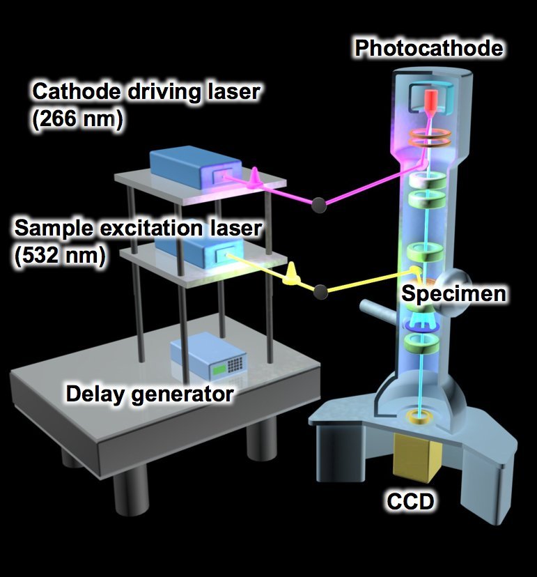
In Ortalan group, to reveal the fundamental properties and the dynamics of the structural and chemical transformations in materials, we utilize the-state-of-the-art Ultrafast TEM (UTEM), Aberration-Corrected and In-situ Transmission Electron Microscopy, Nanoscale Electron Tomography, Electron Energy Loss Spectroscopy (EELS), and modeling techniques such as Finite Element Analsis (FEA). You will find brief descriptions of some of these efforts in our group below.
 Freezing the time: Ultrafast Transmission Electron Microscopy
Ultrafast TEM is a truly unique instrument, which allows to investigate dynamics of materials, such as structural, electrical, magnetic, and optical responses of materials both in real space and in reciprocal space with high spatial resolution and femto to millisecond temporal resolution. Read more →
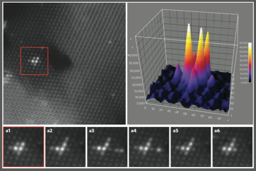
Atomic Scale Quantitative Scanning Transmission Electron Microscopy
With the development of sub-Ångstrom resolution AC-STEM, a quantitative “atom by atom” characterization of materials can be achieved. Especially, Z-contrast high-angle annular dark field (HAADF) mode, in which the image contrast is approximately proportional to the square of the atomic number, is highly useful to determine 3D shape of supported metal catalyst at atom-scale.
Image from V. Ortalan et al., Nature Nanotech., 5 (2010), 843-847.
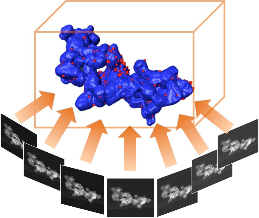
 Nanoscale Scanning Transmission Electron Microscopy Tomography
Since 3D morphologies of nano-materials are highly correlated with materials’ properties, 3D characterization is highly required. With the Z-contrast STEM tomography having 1 nm3 resolution, 3D morphologies of nanomaterials can be quantitatively determined. Read more →
Image from C. W. Han et al., Nano Letters, 15 (2015), 8141-8147.
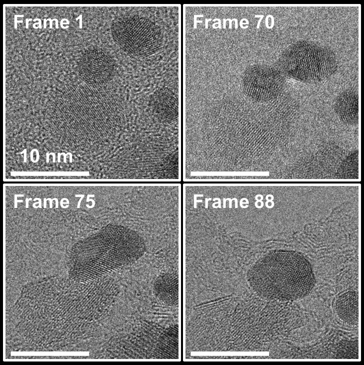
 Probing Dynamics of Nanostructures Using In-Situ TEM
Recent advances in microscopy instrumentation make it possible to investigate dynamic behaviors of materials in real time under external stimuli. By directly observing materials’ dynamics, important questions in materials science can be addressed.

